Background
Reflect array antennas for wake vortex detection radars and weather radars
The successful use of a reflect array antenna within an X-band weather radar will lead to major simplification of the mechanical structure combined with a faster scan cycle. The end result is simpler, smaller, and more reliable than today’s weather radar systems, and which at the same time provides more data. The inherent shortcoming of long-range radars of not seeing beyond the horizon because of earth curvature blockage (and thus not detecting low-altitude weather phenomena a distance apart) is at times addressed by a denser radar network. This approach, however, suffers from the high cost of radars. A low-enough priced X-band radar could fit this need and thus expedite the emergence of dense radar networks. Additionally, there are applications where the long range of a C-band radar is not fully appreciated (e.g. at mountainous areas, local weather watches, and mobile and certain atmospheric research applications). The benefits of the new antenna construction would provide a significantly higher perceived customer value and improve the supplier’s competitiviness. A small enough size would also likely increase the demand for mobile weather radars, and extend their applications beyond the current predominant research use.
A state of the art X-band weather radar antenna has following characteristics:
- Frequency range : 9.3-9.8 GHz
- Beam width: 0.95°
- Gain: >45 dBi
- Highest side lobes: <30 dB
- Cross-pol. isolation: >35 dB
- Two simultaneous orthogonal polarizations with matching radiation patterns
Air traffic will triple in the next 20 years. This increased traffic must not be accompanied by increased accidents, meaning the performance of safety-related systems must be tripled in the 20 years. This improvement must be achieved with all weather operation. Nowadays, conventional aviation weather hazard warning does not meet the pilots need for accurate, timely and spatially high-resolution detection and communication products. Airports capabilities to treat the increase of traffic will rapidly become the bottleneck of the whole transporting chain. The major airports have today to face several types of issues: 1) they approach their ultimate capacity in term of passengers; 2) the delays necessary between the take-off of two succeeding planes is increasing with the size of the plane, due to wake vortex in the drag of heavy aircrafts; 3) the level of safety should be maintained and even increased (wake encounter events could increase in-line with the increase in traffic).
Note that there typically are also smaller lower gain antenna options available for applications which do not need such a high angular resolution, so the gain and beam width values above are only examples. The state of the art weather radar antenna of today is still a traditional parabolic reflector antenna, which is mechanically scanned both in azimuth and elevation. The phased array antennas are only gradually starting to be used also in weather radars. The main reason for this has been the price of the phased array technology so far. A state of the art phased array antenna would fulfill the requirements above, but it would also enable fast electrical scanning in one direction (elevation). This would enable faster measurement of the atmospheric conditions of the whole hemisphere with a single azimuth rotation. The proposed antenna demonstrator is a sub-array of such a larger array (i.e., so it doesn't have to fulfill the beam width and gain requirements. However, the goal for the side lobe and cross-polarization performance is as listed above.
WBG devices for microwave and mm-wave circuits
WBG devices currently yield microwave power performance at least a factor of ten superior to GaAs devices with a comparable noise figure of merit (NFOM). Their unique ability to operate at high temperature environments (> 600 °C) will give the possibility to design self-re-configurable control units for severe operating conditions in a wide variety of applications such as spacecraft and satellite, and also homeland defence, automotive and nuclear power plants. The intrinsic physical properties of wide band-gap materials such as GaN are ideal for the fabrication of high power transistors for microwave and millimetre wave applications. In particular the high breakdown field (~3 x 10⁶ V/cm for GaN) and the high electron saturation velocity (~3 x107 cm/sec for GaN), more than compensate its lower electron/hole mobility, enable the realization of high power, high efficiency microwave transistors in the frequency range 1 to 40 GHz. Moreover, thanks to the large band gap (~ 3.4 eV for GaN) and temperature stability, chemical inertness, very high robustness as well as low sensitivity to space radiation, nitride-based semiconductor materials such as GaN are expected to ultimately show high reliability. For the above reasons GaN technology can be considered as a real “disruptive technology”, capable of significantly reducing the number, size and cost of devices utilized in transmitter and receiver chains of front-end modules used in phased array radars. In particular GaN HEMT transistors and MMICs, on both SiC and Si substrates, have just been developed to operate at microwave frequencies up to 40 GHz. State-of-the-art output power densities currently reach values higher than 20 W/mm at C band (4-8 GHz), and around 10 W/mm at X band (8-12 GHz), about ten times greater than GaAs transistors of equivalent size. Considering such performances, it is foreseeable, once the thermal management problems will have been completely solved and the technology yield and reproducibility improved, to develop solid state HPAs capable of delivering an RF output power approaching 100 W at very high frequency ranges (up to 40 GHz). Consequently, AlGaN/GaN HEMTs may be used in this project for high power amplifier (HPA) and low noise amplifier (LNA) making. In the last case, the material properties make it possible to simplify the circuit avoiding the limiter protection circuitry to present damage to the high sensitivity receive chain. The potential of the very promising AlN/GaN HEMT for power devices will be evaluated.
RF-MEMS based switches, matching networks and phase shifters will dramatically reduce the losses in the T/R module, thus increasing the overall performance of the receiver. Especially for receiver antennas where the received satellite signal is relatively weak this will make a whole world of difference. This is certainly important for the noise matching of the LNA. The frequency range over which satellite receivers should operate can be relatively rather large (e.g. 2-20 GHz). This implies that the noise matching of the LNA is always worse for wider frequency band than for a certain sub-band. With RF-MEMS technology, it will be possible to tune the LNA to a certain sub-band with corresponding noise performance. This also will increase the performance of the satellite receiver front-end significantly. The frequency-agile LNA will be realized using two different complementary approaches using monolithic integration respectively. We will also implement the MEMS matching networks together with the LNA on the same GaN chip to enable a fully monolithic GaN tunable LNA to be realized (for this we will use results obtained for the fabrication of SPDTs on the same chip as HPA and LNA to fabricate in the same way matching networks). At the end, we will be able to the measured RF performance and integration level achieved using this approaches.
General trends for transmit and receive front-end systems
Technological trends for transmit and receive front-end systems for many kinds of applications:
- Communications with narrow and UWB frequency ranges where UWB systems have shown to provide immunity to solid surrounding mode interference;
- Space applications like environmental monitoring and cartography.
We can see that the today GaAs process will be replaced in a narrow future by GaN process for power circuits and also low-noise circuits; concerning the power switches, today we use circulators, which are big, high cost and not available for all applications; so MEMS power switches are mandatory for better integration with lower cost, and sometimes just for feasibility aspects.
Choice of the substrate: GaN bulk, SiC, Sapphire or Si?
GaN substrates (wafers) are not a viable alternative for HEMT devices and circuits due to numerous materials and economical challenges faced by the GaN substrate R&D community and the immaturity of bulk GaN crystal growth. Thus, the deposition of GaN thin films on Si and SiC is the primary approach for the fabrication of GaN RF power devices and circuits.Sapphire is a low cost solution for GaN technology as compared with SiC. However, unlike the GaN-based LED market, the use of sapphire (Al203) as a substrate for RF devices is not the best option due to the poor thermal conductive properties of sapphire compared to that of Si and SiC. Si substrates have low crystal defect density, have zero micropipes or other macro-defects, and offer a high quality surface as required for performing epitaxy. Additionally, the wafer-wafer consistency and quality are unmatched in other materials and are the result of decades of optimization of the manufacturing process of Si substrates. SEMI standard, high resistivity silicon (104 Ohm-cm) substrates are available through the process of zone refining of Si ingots and have very low impurity concentrations. Growth of high quality GaN on Si (111) can be achieved by addressing the significant levels of lattice misfit (~17%) and thermal expansion coefficient (TEC) (~ 56%) mismatch. An initial layer of aluminum nitride (AlN) is deposited on the Si substrate to accommodate the strain associated in differences between crystal properties of Si and GaN. Several groups have made efforts to manage this high level of lattice and thermal mismatch, with varying degrees of success while Nitronex has developed a growth process that results in the growth of crack-free GaN, which has been used to fabricate GaN-based devices in both microelectronic and optoelectronic areas.
SiC on the other hand has the best lattice match to GaN.
Thermal considerations
Another aspect of choosing the appropriate substrate for GaN-based RF products is the thermal conductivity needed to design parts meeting the customers thermal design criteria. Of the two common choices, SiC has a higher thermal conductivity compared to Si. However, the extent of thermal conductivity benefit of SiC over Si is diminished by the following:
- The thermal conductivities of Si and SiC are plotted in figure below. Although SiC is more thermally conducting than Si, the difference in thermal conductivity of SiC over Si diminishes as temperature increases and approaches typical operating temperatures of ~175°C.
- The thermal resistance of the package contributes ~50% of final thermal resistance of the packaged device. Therefore, the contribution of the substrate to the final thermal conductivity is reduced.
- The power amplifier application specific thermal resistance targets are also met through die thinning. Nitronex has achieved ~15% reduction in thermal resistance by reducing GaN HEMT on Si die thickness from 4mils to 2mils.The benefit of SiC when compared to Si diminishes as die thickness is reduced as shown in a figure below. The temperature rise of GaN devices show reduced sensitivity to substrate thermal conductivity as die thickness is reduced. For the purpose of comparison, a 10 finger device with 200Mm gate width and 25μm gate-gate pitch was simulated with a dissipated power of 3W/mm on both substrates
|
|
|
|
Thermal conductivity over temperature for Si and SiC |
Temperature rise of GaN devices show reduced sensitivity to substrate thermal conductivity as die thickness is reduced. |


Processing considerations
The availability and maturity of back-side processes for a silicon substrate provides the opportunity for performing source via interconnects with commercial-off-the-shelf processes and equipment. The ease of thinning also negates the intrinsic thermal conductivity advantages of a SiC substrate by allowing for aggressive and advantageous thermal engineering solutions leveraging the low cost structure of silicon solutions. The availability of high thermal conductivity die-attach techniques that have been developed for silicon are now directly and easily applicable to GaN-on-Si technology.
Cost considerations
RF power transistors and circuits represent a significant cost of amplifiers used in both commercial and military applications. Therefore, the cost of the substrate is critical for PA applications and has an impact on final cost of the device. The cost of the RF component is dependent on substrate cost, processing costs and yield costs as discussed in greater detail below.
- Substrate cost: The cost of a 100-mm diameter high resistivity Si substrate is ~$30-60/wafer in volumes required to satisfy all identified applications of RF power transistors. High resistivity 100-mm (4H variety) SiC substrates are not readily available in volume for purchase and are reported only in R&D quantities of a few wafers.3-inch diameter SiC wafers are reported to be available at a cost of ~50-100 times the cost of a 100-mm Si substrate. The maximum volume of 4H SiC that is obtainable is largely unreported and is assumed to be in R&D quantities.
- Processing costs: GaN HEMTs are processed in low volumes. Therefore, the processing cost per wafer will be likely dominated by fixed costs. Thus, the processing costs for 100-mm Si and 3-inch SiC wafer can be assumed to be the same.
- Yield costs: Die yields affect final cost significantly because high back end costs in packaging, assembly and test cost are incurred. In case of power amplifier modules, the back end cost for a single amplifier can be hundreds of dollars. GaN MMIC PAs may occupy large areas (up to 50mm2 per MMIC), requiring very low defect density to produce high yields. Use of Si substrates improves chips/processed wafer in three important ways. Firstly, a 100-mm wafer Si wafer is 180% the area of a 3-inch SiC wafer for an edge exclusion of 3-mm. Thus, the number of devices per wafer is increased enabling substantial cost reductions. Secondly, SiC substrates contain micro-pipes and other wafer imperfections, which are yield killers, while Si wafers are free from such macro-defects. Thirdly, the larger wafer area reduces edge exclusion effects during epitaxy and processing leading to increased number of chips/wafer. It is difficult to precisely compare the cost of devices from GaN/Si with GaN/SiC. However, by making some assumptions, Nitronex has estimated the cost benefit of using GaN/Si over GaN/SiC. The key assumptions are: 1. The cost of fabrication for GaN/Si and GaN/SiC is assumed to be the same. This includes front and backside processing. 2. The yields for all GaN/Si and GaN/SiC are assumed to be identical for a given volume of wafers. However, as discussed earlier, this assumption underestimates the cost of GaN/SiC due to impact of micro-pipes.
|
|
|
Estimated cost of GaN/SiC vs. GaN/Si for two different wafer sizes. The estimated costs for 150-mm GaN/Si and 3 inch GaN/SiC are normalized to the cost of 100-mm GaN/Si for comparison |
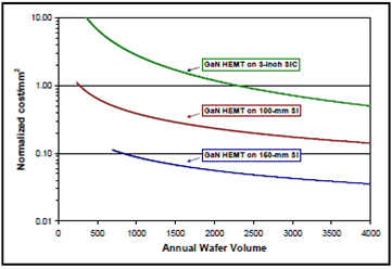
This estimation is shown below. The cost/mm2 was calculated for 3-inch GaN/SiC, 100-mm GaN/Si and 150-mm GaN/Si. Then, all the costs are normalized to the cost of 100-mm GaN HEMTs for purposes of comparison. It can be seen that the cost of GaN/SiC is S3x the cost of 100-mm GaN/Si due to half the area and substantially higher substrate costs for volumes S 3,000 wafers per year. For Si substrates, scaling the wafer diameter from 100-mm to 150-mm has further potential to reduce costs of GaN HEMT die. The other important aspect of substrates for GaN HEMTs is the availability. It is conservatively estimated that 2500-5000 100-mm wafer equivalents of discrete devices are required annually to satisfy the power amplifiers for the commercial wireless infrastructure market. The military applications will likely require an additional 25-50% of 100-mm wafers equivalents. The usage of large area, high power GaN MMICs instead of GaN HEMT discrete devices further increases the number of wafers required to meet the demand. Thus, it is not only important to understand the cost of the GaN HEMT wafer, but it is also essential that the required supply of substrates for GaN can be secured to satisfy the high volume applications.
Thus, SiC provides the possibility of material quality improvement due to better lattice matching conditions, as well as better thermal conductivity. While the best power performance reported for GaN-based HEMTs is from device layers grown on SiC, the use of Si substrates allows for greater ease of backside processing while allowing good thermal management. The high cost and the small SiC wafers’ dimension represent a severe obstacle to overcome in the research phase. In order to guarantee low cost 3” inch wafers, mandatory condition to optimize a real production capability for RF-MEMS, GaN growth over sapphire or silicon substrates are commonly employed. In fact thin film technologies that are optimized for RF MMICs could be considered practically independent from the substrates properties and, furthermore, many RF applications are not drastically changed if SiC is substituted with low cost material. Nevertheless, SiC substrates represent the best choice in reason of its physical properties and particularly for the very high thermal conductivity, chemical stability and radiation hardness. Taking into the account the above discussed features and considering the fact that NANOTEC faces an additional challenge due to the extra desire for GaN-based material compatibility for RF-MEMS and MMICs, we propose that RF-MEMS and MMICs will be studied on silicon and SiC substrates by TRT and FORTH. This choice was made based on existing expertise and technology availability. Results on substrate choice obtained from RF-MEMS/MMICs will be compared and the conclusions drawn will be used for selecting preferably a single substrate for all components envisaged under NANOTEC, thus establishing a common substrate reference (SiC) for comparison at each fabrication line.
RF-MEMS
Circuit tunability and re-configurability are nowadays essential to satisfy most of commercial and professional telecommunication system requirements. Intelligent micro-systems must handle functionalities such as signal routing, variable impedance matching, adjustable gain amplification, tuneable phase shifting, etc. To this end, RF-MEMS appear to be the future winning technology. Today, designers of antennas and receivers with high power controllable devices (phase-shifters, switches, etc.) must choose among the following switching solid-state technologies: Ferrite phase shifters offer the lowest RF insertion losses. Unfortunately these devices are bulky and very expensive, and need expensive control circuits to manage their temperature behaviour. PIN diodes are low cost devices, but insertion losses are still high compared to ferrite, and the polarization current must be kept high to reduce the series resistance (and the insertion losses). It is thus apparent that the realisation of miniaturized MEMS with low switching time, high reliability, high power handling, low insertion loss and low cost of fabrication will be of primary interest for many applications .
In order to achieve the expected results and to realize Intelligent Micro-systems on GaN materials satisfying both commercial and professional (space/defense) requirements, specific enabling technologies have to be developed. In particular, circuit re-configurability, as well as switching of the electrical signals are required in any intelligent microwave and millimeter MMICs, for signal routing, variable impedance matching, adjustable gain amplification, tunable phase shifting, etc. To this end, RF-MEMS appear to be the future winning technology. Low power RF MEMS switches display excellent RF characteristics, including insertion loss below 0.2 dB and isolation higher than 25 dB up to 40 GHz, negligible consumption and improved inter-modulation performance. When applied to a monolithic X-band (10 GHz) phase shifters, Raytheon has demonstrated a 4-bit monolithic MEMS device with insertion loss reduced to 1.7 dB in all states, compared with 6-7 dB of the best pHEMT GaAs devices. As miniature relays, low power RF MEMS offer large advantages in terms of size (typically 120 x 300 µm²/switch), power consumption (typically 1,5 µW/switch) and cost: the area and volume of RF subsystems can be reduced by about 50 %, compared to the conventional PIN technologies. In recent years, low power RF-MEMS now being offered from companies in the US, In fact, large quantities of packaged low power RF-MEMS switches have been successfully integrated into a practical RF system (e.g. 25 000 Radant MEMS switches were used within an electronically steerable antenna ). TRT RF-MEMS switches also recently demonstrated remarkable RF-power handling capabilities, with more than 6 W RF-power under hot-switching conditions.
Phase shifters
Next, we will present a summarized description of the global state-of-the-art with respect to phase shifters. Front-end circuits like filters, matching and phase shifting circuits are key components in many RF systems. A lot of research has been made within this field, especially during the last decade or so. Modern radar and communication systems have created a need for finding novel RF front-end solutions that can result in a reduced complexity and potentially also lower cost. Traditionally, tunable front-end filters have been realized as non-planar filters that are bulky and the size and weight of such filters limit their use in highly integrated RF systems. In terms of planar filters, solid-state (p-i-n diode or transistor) based varactor-tuned filters are much smaller in size but the relatively high losses and low linearity of such filters have been limiting factors for a wider use in wireless RF systems. A disadvantage with using p-i-n diodes as filter tuning elements is that they will consume relatively high levels of DC power which also can be a limiting factor in many systems. Better performance can be achieved with RF MEMS (compared to solid state technology) and it has already been applied to filters, matching networks and phase shifters. However, to be able use such types of MEMS based circuits in real systems further improvements are needed with respect to performance, reliability as well as achieving low cost. A key problem for the integration of RF MEMS circuits is packaging and this may be done at wafer level to lower the cost. By integration of MEMS into RF subsystems, a higher degree of functionality would be possible, for example in reconfigurable antennas, filters and amplifiers (e.g. in reflect-arrays and tunable filters).
Reflect arrays
Reflect arrays can be said to combine some of the best features of the conventional printed phased array and parabolic reflector antennas. Reflect arrays are much less expensive than standard phased arrays and provide ample space for drivers and receiver electronics. They are space fed; therefore, they do not suffer from the high transmission-line (corporate feed) loss as the array size increases. The individual elements of the array are designed to scatter the incident field while impressing the appropriate phase shifts in such a way as to form a plane wave-front that propagates in a prescribed direction or, more in general, to create the required radiation pattern. The elements of the array can be microstrip patches or waveguide apertures, operating on linear, dual or circular polarization. The phase shift needed in order to synthesize the scattered wavefront adaptively can be achieved in many different ways (i) by varying the geometry of the radiating elements or its electrical properties using tuning device within the radiating elements, or (ii) using tuning elements that are separate but EM coupled to the radiating element. The tuning elements can be e.g. PIN diodes and RF MEMS. This is an application where the inherent advantage of using RF MEMS technology lies due to their low power consumption, high linearity, low loss, and high isolation.
Reflect arrays – Progress beyond state of the art:
The RF MEMS can be integrated into the antenna design to achieve a higher degree of functionality for the reflect array. Results has shown that that it is possible to design a reflect array with large beam scanning (+- > 63 degrees) and excellent performances in gain (22.2 dBi for = 0° beam squint), cross-polarization (£27 dB) and side lobes level (£10 dB). Novel solution in order to reduce the sidelobe level and improve the cross-polarisation according to the specifications will be evaluated in NANOTEC by combining knowledge design of unequally spaced reflect-arrays using fixed tuning for the elements with RF MEMS tuning of the elements. Unequally spaced reflect array has shown to have lower sidelobe levels and increased gain in relation to conventional reflect-arrays. In the design of the reflect arrays the following critical issues have to be taken into account: (i) to achieve low loss in the tuning elements (can be achieved using RF MEMS) and in the antenna elements (using low loss or micromachined material), (ii) find collective mounting solutions and packaging for the combination antenna – tuning elements. For achieving low cost, a global and repetitive process shall be defined, which includes packaging, RF MEMS, substrate, RF layers and DC board.
Integration of RF-MEMS and active RF devices
Today, there is an increasing interest in making RF-systems self-adjusting or "cognitive". Realization of more “Intelligent Microsystems” could result in a paradigm shift in RF component design since such highly flexible micro-systems will have the ability to optimize their performance over broad bandwidth, overcoming the trade-offs that current RF components must endure. For end-users that may have different and also changing demands, following such an approach will allow a higher degree of flexibility (compared with today’s existing solutions in where the over-all system performance is largely controlled by the manufacturer). Such a unique ability is expected to lead to very efficient RF systems with reduced size, weight, power and cost (due to facilitating component re-use and achieving further miniaturization compared with using conventional technologies). Frequency-agile (adaptive) front-end architectures realized using SiGe, GaAs/GaN MMIC processes with embedded RF-MEMS switches are enabling technologies proposed to achieve those highly attractive benefits. By monolithic integration of RF-MEMS and MMICs, a higher degree of functionality would be possible, e.g. in active reconfigurable (multi-band or switched wideband) antenna front-ends. Hybrid integration using bond-wires is not feasible for many demanding mm-wave applications (such as upcoming 94 GHz/140 GHz imaging systems) requiring monolithic integration.
Integration of RF-MEMS and GaAs/GaN based active RF devices
Most of the research work carried out to this date, however, has lacked much real demonstration of monolithic integration of active circuits and MEMS switches above 5-10 GHz or so (i.e. on the same chip thereby enabling a higher level of integration and improved RF performance to be achieved). RF-MEMS together with active RF-circuitry have so far (with a few notable exceptions) mostly been realized as hybrid circuits and mainly up to 5- 10 GHz which still leaves room for significant improvements to be made with respect to RF-performance, frequency range, functionality as well as to achieve reduced complexity and lower costs. Intelligently controlled L-band and X-band GaAs PAs using off-chip (wire-bonded) reconfigurable RF-MEMS based output tuners. A 3-9 GHz frequency-agile GaAs amplifier with a tunable MEMS input matching network connected using bond-wires. The X-band switched dual-path PAs and LNAs reported by the US company Rockwell Scientific are the first real examples of a successful monolithic integration of active devices with RF-MEMS switches in a GaAs MMIC foundry process also demonstrating enhanced circuit functionalities.
A 20-30 GHz single-chip MEMS switched LNA MMIC has very recently been successfully fabricated and tested. RF-MEMS SPDT switch network (together with other fabricated MEMS test circuits) made on a GaAs MMIC wafer that has been combined with two commercially available (COTS) GaAs C-band (4-8 GHz) LNA chips using wire-bonding. The measurement results showed that this GaAs MEMS based reconfigurable (switched) LNA front-end circuit achieved a 30 dB difference in in-band gain and attenuation (when one of the MEMS switches used were turned on and off, respectively) while also being able to maintain a similar high gain (low NF) and linearity in comparison with the standard (fixed) LNA MMIC that was used. Small-signal and large-signal characterization have also been carried out on a corresponding GaAs MEMS switched LNA hybrid circuit realized using a 1-47 GHz (COTS) LNA MMIC. While this particular wire-bonded GaAs MEMS switched LNA device has demonstrated reconfigurable gain, high linearity and low NF over a very wide frequency range the results also highlights the possibilities and benefits of monolithic integration of MEMS switches and active RF devices on the same GaAs substrate, especially within the mm-wave range.
In spite of the recent remarkable progress in microwave and millimeter-wave applications of WBG devices, no results have been reported so far on a reconfigurable RF-MEMS based switched amplifier (LNA/PA) on GaN/SiC substrates. This is also in spite of the acknowledged superior RF properties of such enabling technologies (e.g. in terms of very high power efficiency and low-loss low-power switching) that should make them ideal candidates for use in future Intelligent Micro Systems (IMS) applications. Selex recently reported on a first successful demonstration of RF MEMS switches and active RF circuit function blocks (e.g. LNA) fabricated on the same GaN wafer. Experimental data of such GaN based RF MEMS switches and fixed (i.e. not reconfigurable) LNA circuits showed capabilities for monolithic integration with promising results. It is evident that a successful combination of GaN MMIC amplifiers and high-power MEMS switches, as targeted within this proposal, would enable new types of RF components with unprecedented performance. Such types of components could preferably also be realized monolithically, i.e. on a single chip to avoid a use of lossy off-chip interconnects such as bond-wires and result in further miniaturization and improved performance. Moreover, specific research programmes are being dedicated to optimize power performance of GaN-HEMT devices with the aim to develop a stand-alone European supply chain and capability for GaN technology. Leading European research labs and foundries are already involved in this research, such as TRT, involved in the KORRIGAN Consortium (European initiative for GaN HEMT technology). To reduce as much as possible the time and cost of technology development for RF-MEMS, it is necessary to consolidate the thin film technologies already employed for GaN MMIC fabrication in order to identify a process flow suitable for RF-MEMS integration.
Integration of RF-MEMS and silicon based active RF devices
The rapid growth of the wireless communication market up to 100 GHz and beyond during the past years has been a driving force for the development of adaptive multi-band RF front-end systems. These systems are required to cover multiple frequency bands and operate under different power levels for various standards and applications. Reconfigurable impedance matching networks capable of electronic tuning are one of the key components in the development of adaptive RF front-ends. Some first examples of monolithically integrated (i.e. single-chip) RF-MEMS enabled reconfigurable CMOS amplifiers have recently been demonstrated at frequencies up to 5 GHz using post-processing steps. A K-band CMOS PA combined with an off-chip MEMS tunable bandpass filter. The combination of low-loss RF-MEMS switches and SiGe/CMOS technology will enable novel types of reconfigurable circuits (e.g. frequency-agile LNA/PA) of high importance for future low-cost flexible RF systems. FOI and UU have designed reconfigurable MEMS matching networks made on quartz and silicon substrates and combined those ones with 24 GHz SiGe LNA chips (CAS2009 Best Paper Award).
Si/SiGe BiCMOS RF-MEMS technology
The latest developments in SiGe technologies provide very fast Heterojunction bipolar transistors (HBTs) for mm-wave circuits. The consortium partner IHP Microelectronics presented a SiGe BiCMOS technology with the fmax values of 500GHz in IEDM 2010, as a world record. Such high fmax values let the designers to realize RF circuits with an operating frequency of more than 100GHz. High frequency systems also need special requirements such as multi-band/wide-band operation, phased-arrays and etc. RF-MEMS switches are considered as the key components to fulfill these requirements of mm-wave applications. For such high frequency applications, a monolithic, embedded integration of the switch with a high-performance CMOS or BiCMOS platform would be advantageous over any heterogeneous integration with the basic IC process because it provides shortest connection paths between switch and circuitry resulting in lowest parasitics. Last year, consortium partner IHP announced a BiCMOS embedded RF-MEMS switch for mm-wave applications in IEDM 2009. The details of the IHP’s 1st generation RF-MEMS switch are given below.
|
|
|
|
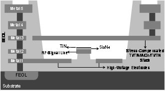
IHP’s 1st generation RF-MEMS switch integration scheme and SEM picture. The RF-MEMS switch is embedded to IHP’s 0.25µm BiCMOS process Back-End-of-Line (BEOL). |
|
IHP’s 1st generation RF-MEMS switch is a convenient solution for the requirement up to 90GHz with a low insertion loss (<0.7). The developments and the optimizations on IHP’s 1st generation RF-MEMS switch showed that the integration technique is very promising from reliability, repeatability and the yield issues and can be offered as a BiCMOS process module. The 1st generation RF-MEMS switch technology is already in use by several groups in Europe and is becoming more mature day by day. However, for the applications at 90GHz and beyond, the relative high insertion loss of the 1st generation RF-MEMS switch (>1dB) limits the usage of the technology. Furthermore, the packaging of these switches is also one of the main issues for the commercialization of RF-MEMS technologies. The required cap-to-wafer packaging techniques are relatively expensive and not suitable for mass production. Wafer-to-wafer packaging method would be a real solution to decrease the cost of the developed technology. IHP microelectronics recently announced in IEDM 2010 conference a new RF-MEMS switch integration technique as the 2nd generation RF-MEMS switch which provides an embedded RF-MEMS switch for 90GHz and beyond with a insertion loss of less than 0.5dB. The special integration method of 2nd generation RF-MEMS switch also provides wafer-to-wafer packaging. The wafer-to-wafer packaging of 2nd generation switch is also developed by the consortium partner, Fraunhofer IZM. The switch integration is very simple, adding only one mask step to the underlying high-performance BiCMOS process. No performance degradation was observed after 5 billion cold switching cycles demonstrating the high reliability of the IHP’s 2nd generation RF-MEMS switch.
The second important issue is the stabilization of the developed RF-MEMS process. During last decades, several RF-MEMS switch have been demonstrated in literature but stabilization and the repeatability of these technologies were poor. IHP Microelectronics has continues operating clean-room and has several qualified BiCMOS pilot lines in the technology nodes of 0.25µm and 0.13µm. IHP has significant experience on the stabilization and the qualification of various different technologies which can be used to stabilize the developed RF-MEMS technologies. The third main issue for the commercialization is the modeling/Design-Kit issue. Even the technologies become stable, offering the RF-MEMS technology with an appropriate Design-Kit needs special effort. Moreover, BiCMOS embedded RF-MEMS switches requires models which should be integrated to foundry technology libraries and Design-Kit of the technology. By the integration of the model to the Design-Kit, all the consortium partners can access to the technology and perform simulations together with all other library components, such as HBTs, MOSFETs, capacitors and etc. The consortium partner Coventor has experience on modeling of the MEMS devices and Coventor is working on a new concept called MEMS+, which allows performing MEMS device simulations together with foundry models. By using the new co-simulation concept, developed RF-MEMS switch models can be simulated together with other components in same well-known environments, such as Cadence and Agilent ADS. Last point regarding the bottlenecks of the RF-MEMS technologies is the reliability of the technology. A special effort on reliability of the RF-MEMS technology is given to IHP’s 1st generation RF-MEMS switch and several optimizations/developments are still on-going. A special reliability test method also developed by IHP Microelectronic and applied to the 1st generation of IHP RF-MEMS switch. The developed method uses Laser-Doppler Vibrometry on a semi-automated probe station to perform the automated reliability tests in parallel to several structures and the technique detects not only the failure but also time-dependent degradation of the RF-MEMS switches. Using the developed method, potential stictions/failures can be predicted. Moreover, by using the same method packaging requirements can be extracted for safe operation. The first test results shows that the IHP 1st generation RF-MEMS switch provides more than 50 Billion switching cycles without any performance degradation. The results were presented in SiRF 2011 conference.
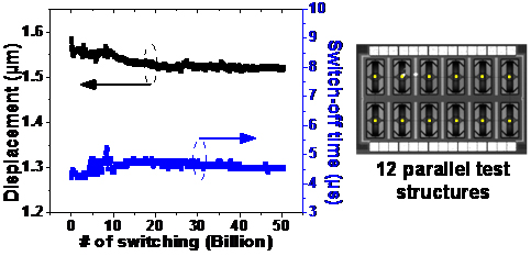
Membrane displacement and switch-off time vs. number of switching cycles for all 12 single switches.
The intended multifunctional SiGe BiCMOS RF-MEMS chip operating at 140GHz includes complete transmit/receive functionalities, up- and down-conversion and digital circuitry to address the different building-blocks by a daisy-chain like BUS architecture.
The multifunctional chip will feature multi-channel capability, in order to drive several antenna channels at the same time for the MIMO method. For the antennas, two solutions are foreseen in the project: external antennas and on-chip antennas. The latter ones have the advantage that no RF-interconnection at 140GHz is needed to realize the system. The on-chip antennas will be realized by back-side etching of the substrate.
In summary, the 140GHz chip will have the following advanced features:
- Complete transmit and receive functionality on chip including up- and down-conversion (SiGe devices)
- High-performance transmit/receive switch (RF-MEMS device)
- Digital BUS interface for addressing of the building-blocks (BiCMOS device)
- On-chip antennas and high-Q passives
Combination of RF-MEMS and semiconductor technology
The combination of MEMS and semiconductor technologies has been a very popular research topic for the last several decades. Several methods in literature were suggested to integrate MEMS components into semiconductor die using hybrid, monolithic, and post-processing techniques. The processing techniques in MEMS and semiconductor processes are similar but low throughput, difficult repeatability and low yield of MEMS processes makes this combination very difficult. Moreover, the high yield requirement which allows decreasing cost in semiconductor technologies are highly threatened by integrated MEMS devices. All these bottlenecks force the industry to find an intermediate solution, such as heterogeneous integration. In these days, the chip stacking using Thru-Silicon-Vias (TSVs) and the interposer techniques become popular to combine different dies together. By using these methods, different products are already in market which includes several MEMS components. The interconnect losses from these integration methods are in acceptable range for the frequencies lower than 40GHz. But, for the frequencies above 60GHz, the interconnect losses become much more important and defines the overall system performance. Due to the big effect of interconnect losses in interposer or chip stacking techniques, embedded integration of RF-MEMS components into the semiconductor technologies are necessary especially above 60GHz applications. According to ITRS 2009 Roadmap, MEMS embedded integration with IC is also required to be available by 2012. For the time being there is no solution yet. Such fully embedded solutions at higher mm-wave frequencies become increasingly attractive as applications with substantial market volume surface, such as 60 GHz personal area networks, automotive radars in the 76-81 GHz range, or security radar/imaging at 94 GHz and 140GHz radar systems.
The latest developments in RF-MEMS technology have paved the way for achieving high performance and IC-integrated components, especially RF-MEMS switches and high-Q passives. RF-MEMS switches seem to be the key component for the development of the next generation reconfigurable/multi-band communication circuits while MEMS based, high-Q on-chip passives components can improve the performance of mm-wave circuits significantly. Further, publicly funded projects are going on (or are about to be started) considering the monolithic integration of RF-MEMS with GaAs semiconductors (FP7 ICT project: MEMS4MMIC) and with GaN-semiconductors (FP7 Space project: Saturne). But, in contrast to the NANOTEC objectives, these projects are targeting high-end niche markets, because underlying technologies are expensive, with limited wafer sizes and little potential for production scale-up. Additionally, the complexities of the ICs in both projects are limited to RF-MEMS switch functionalities combined with amplifiers based on the semiconductor transistors. NANOTEC on the contrary is exploring a low-cost semiconductor technology, suitable for the mass-market, scalable to large wafer sizes, and offers a variety of functionalities on chip, like
- RF-MEMS switches
- SiGe multi-functional ICs combing amplifiers, vector modulators, mixers
- Silicon-based sensors (temperature, power...)
- BiCMOS mixed signal circuitry (A/D converters, Daisy-chain interfaces)
- Potentially: Charge pumps for achieving the high necessary actuation voltages of RF-MEMS switches using special high-breakdown p-channel MOSFETs.
Size reduction
The innovation of the project relies on the highly reduced dimensions (150 times smaller) of the miniaturised MEMS switched capacitor compared to the standard shunt capacitive device. The advantage of reducing the size is to improve the mechanical behaviour by increasing the spring constant, the restoring force of the beam and by reducing temperature dependence. A smaller device results in a higher mechanical resonant frequency and faster switching time: typically 200 ns for an actuation voltage around 30 V. The standard MEMS device is completely dominated by the residual stress component while it is less than 30% of the total spring constant for the miniature MEMS device. This leads to a better mechanical and thermal stability of the movable membrane. Since it is always easier to control the dimensions and the deposition thickness of a thin-film layer than its residual stress properties, the miniature MEMS device results in a much more repeatable fabrication process than the standard MEMS device. Miniature MEMS are much more stable in temperature that the standard MEMS device and can be packaged under high-temperature conditions. Miniature MEMS device can withstand a charge density of typ. 2,5.1012 cm-2 before failing in the down-state position. In contrast, the standard MEMS device can only withstand 4.1011 cm-2 . A charge density of 2,5.1012 cm-2, which is fully populated with electrons at the dielectric–air interface layer results in an electric field of 0.66 MV/cm in the dielectric layer . This field is not high enough to break down the dielectric layer. Electron migration in these devices does not limit the power-handling capabilities. The limiting factor is the rms voltage between the MEMS beam and the bottom electrode, which can cause self pull-in or latch-down. 5W of RF power before latch-down is not an issue.
Nanostructured Materials
The aim of nanostructured dielectric development is to reduce the major failure mode of stiction due to dielectric charging in RF-MEMS capacitive switches. Different new nanostructured dielectric will be developed, such as:
- PZT thin layers with improved performances in term of the electrical conductivity
- Aligned carbon nanotubes within a Si3N4 dielectric matrix
An additional aim of the nanostructuring of materials is the development of miniaturized III-Nitride cantilevers for actuators and the realization of nanoparticles on the surface of widebandgap semiconductors for enhancing the catalytic decomposition of gases up to very high temperature sand in the presence of harsh environments, which is a unique feature of nitrides not possible with other traditional materials available so far.
Radar/millimetre-wave/THz imaging for security applications and inspection, DAT (Defence against terrorism)
The following subsection is intended to give a short overview of existing products, prototypes and technologies for security applications using mm-wave and THz based imaging and detection technologies. As described in the following subsections, some of the GaAs and SiGe technologies to be developed in this project are to be demonstrated for this type of application. The possibility to remotely screen people and goods, without exposing them to hazardous X-rays has triggered a lot of product developments and prototypes especially focused on portal-scanning units for primary or secondary person screening
94GHz is the most common operating frequency for the passive systems. This is because the current, commercially available and operationally and technically feasible state-of-the-art receiver technology is at this frequency. The passive and active MMW imagers apply either a mechanical or an analogue electrical scanning principle. The scanners of QinetiQ, ThruVision, Smiths, Brijot and Alfa Imaging use a MMW lens system in combination with rotating or tilted mirrors to focus the beam on a detector and scan the target. L3-COM´s “holographic imager” is based on a hybrid solution of cylindrical mechanical scan and digital imaging, and it claims to be the market leader with several hundreds of systems already installed at airports all over the world. The development phase probably dates back to developments at Pacific Northwest National Lab (operated for Battelle-Institute) in the 1990s.
Early in 2009, Smith Heimann presented its latest approach of an active mm-wave imager, the panel like “eqo” system. It consists of a planar programmable RF-lens. Sago Systems has developed an analogue electrical scanning principle, based on a leaky wave antenna array and many Rotman lenses. The system scans the target in one dimension with different frequencies, performed by a leaky wave antenna. The second dimension is scanned by Rotman lenses as phase processors, connected to the antenna array. Millivision has also presented a purely passive imager solution avoiding any mechanical scanning. It is mainly based on a 2-dimensional focal plane array of low-noise radiometer-frontend modules and person sized mm-wave optics. A quite different approach is followed by the QinetiQ passive THz standoff-detectors SPO that have no imaging capability. They compare the THz emissivity of two single reference points on a suspected person. However, in contrast to the previous equipment described, this can be achieved from 10 to 20 m stand off distance, an interesting capability for certain applications. There are also lower cost radar based products operating at 10GHz that claim stand-off detection of suicide bombers by polarimetric effects. However these non-imaging solutions cannot detect explosive- or ceramic-based threats.
Limitations of present systems
Several limitations of the present technologies are preventing a much wider usage of such mm-wave imager technologies:
- The current sensitivities of the passive systems have room for improvement, which in turn will increase the detection capability of these systems.
- The current receiver prices make the total system price prohibitive for certain markets – thus the cost reduction of the receiver technology will increase the applicability of these systems. This applies to the mechanically scanned systems that use receiver arrays, and to an even larger extent to the electronically scanned imagers.
- The operating frequencies of present systems between 10 and 100 GHz result in rather large physical apertures to achieve image resolutions in the cm range and thus prevent much more efficient and smaller handheld mm-wave imager solutions.
- Mechanical scanning approaches, with their burden concerning maintenance, noise and weight often stops acceptance from the application side.
In addition, the ubiquitous availability of small video-cameras and the emerging access to and affordability of IR and thermal imagers raise a desire for small camera-like units exploiting the very specific features of mm-wave imaging.
94 GHz passive imaging front-ends and progress beyond the state-of-the-art
Radiometer imaging arrays have the potential to provide reasonable quality images through various obscurations that are problematic for IR and visible imaging sensors. Penetration of mm-wave energy through barriers such as clothing, fog, dust, and some building materials has made mm-wave imaging a promising method for concealed weapons detection, all-weather vision, and through the wall imaging of building interiors. The trend in recent years has been towards antennas where each antenna element is an antenna integrated receiver following the idea of having a “radiometer on a chip”. Some early developed radiometers for the mm-wave frequency band used Schottky diode detectors directly following the antenna which gave a noise equivalent temperature difference (NETD) that was often not high enough for the imaging sensitivity to be useful in a realistic scenario. In recent years zero bias diode detectors have been developed having very low 1/f noise which alone or combination with low noise InP MMIC amplifiers can give NETD values of 0.3–0.5K that are low enough to be useful in some realistic applications. Assuming further that a low-loss Dicke switch in combination with an LNA and a synchronous demodulator (synchronised with the switch) is in the radiometer chain the gain variation over time for the radiometer receiver can be cancelled and the resolution (or sensitivity) will be the inverse function (square root) of the bandwidth (BW) and the integration time () of the integrator in the radiometer times the system noise temperature (or noise figure) of the complete receiver front-end (Ts).
A compact 94 GHz 4-channel Dicke switched passive imaging radiometer employing a mechanically scanned focal plane array was recently presented in. A receiver MMIC with an NF of 4 dB and gain of 10 dB at W-band were used in each channel. Commercial (off-chip) SPST PIN-diodes were used also to form the Dicke switches (having 2 dB of losses) and the additional switch losses also will add to the noise figure of the switched receiver chain (resulting in a total NF of at least 6 dB or so in this case). A recent study presented a comparison of some state-of-the-art mm-wave switches including a GaAs mHEMT based SPDT switch with an insertion loss of 2 dB at 94 GHz and RF-MEMS based SPDT with a loss of 1 dB at 60 GHz. The GaAs foundry OMMIC has further developed low-loss RF-MEMS switches that can be monolithically integrated (i.e. on-chip) using their standard MMIC process technologies and also result in 1 dB of transmission losses at W-band. In this project, we propose to use OMMIC’s state-of-the-art 70 nm mHEMT MMIC process with on-chip RF-MEMS switches in order to be able to reach an NF of 3 dB for a 94 GHz GaAs single-chip MEMS-MMIC based Dicke switched radiometer front-end. Compared with using existing GaAs/InP MMIC technology (and without a use of RF-MEMS switches) this may then correspond to an expected improvement of the over-all NF for a 94 GHz Dicke switched radiometer front-end of at least 3 dB. A small antenna can also be integrated on-chip, something that will further increase the level of integration (i.e. RF-MEMS switched antenna front-end) and also avoid a need for using lossy off-chip interconnects such as bond-wires. To be able to further increase the integration level and also reduce the cost, some state-of-the-art silicon based (SiGe/CMOS) 94 GHz Dicke switched radiometer front-ends have recently been presented. The overall NF of those 94 GHz switched receiver front-ends are in the order of 10-12 dB (i.e. showing a switch loss of 3-4 dB together with an LNA NF=6-8 dB). To push the performance of such 94 GHz silicon RFIC based switched radiometers further beyond the current state-of-the-art we propose also to use the very low-loss RF-MEMS switches developed by the foundry IHP (with maximum 0.5 dB of losses up to 140 GHz for such SPST switches) in combination with their advanced 0.25 m SiGe process technology providing an fT=180 GHz and fmax=220 GHz. This is expected to enable SiGe RF-MEMS based SPDT switches with around 1 dB of losses at W-band. Via monolithic integration of such low-loss SiGe MEMS Dicke switches together with an LNA with a target NF of 6-7 dB (and including also detector circuitry on-chip) it could be possible to reach NF=7-8 dB for a 94 GHz SiGe RF-MEMS Dicke switched receiver front-end. This would correspond to a 3-5 dB improvement in NF compared with the state-of-the-art using low-cost silicon technologies.
The GaAs RF-MEMS Dicke switched radiometer receiver MMICs resulting from this project are expected to have a much higher sensitivity than the current technology, thus the quality of the mm-wave images will improve, which in turn increases the detection capability of the system. The SiGe RF-MEMS switched receiver MMICs resulting from this project are expected to have a significantly lower cost than the ones currently available, which will significantly decrease the total system cost (as an array of receivers is used), facilitating sales. As a part of a system simulation study we will also investigate possibilities to further reduce the size and complexity of passive imaging systems (that today are using mechanical scanning) by using electronically scanned antenna arrays.
140 GHz frontend circuits
Monolithic microwave integrated circuits (MMICs) for operation beyond 100 GHz are, with very few exceptions, still the realm of group III-V semiconductors. Due to the progress especially in metamorphic HEMT technologies, they can reach considerable complexity. Using a metamorphic HEMT technology with gate length Lg=100 nm, researchers from Chalmers University, Gothenborg, and Fraunhofer Institute of Applied Solid-State Physics, Freiburg, realized a multi-functional receiver chip for 220 GHz applications.
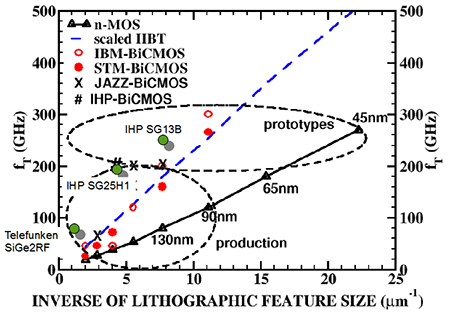
Comparison of ultra-scaled CMOS and SiGe HBT technologies with respect to fT.
The envisioned complexity of the circuits to be used in the 140 GHz MIMO RADAR demonstrator in NANOTEC, however, will not be feasible for implementation using group III-V semiconductor technologies, but requires a Silicon-based process. While it is expected that CMOS circuits below the 65 nm node will be able to deliver the necessary performance, SiGe HBTs can deliver comparable or better performance even at 250 nm minimum feature size. This is shown for the case of transit frequency in the figure above. For comparable transit frequencies, SiGe HBTs will also have the higher breakdown voltages, which is an important issue for RF analogue circuits. The feasibility of circuits with operational frequencies beyond 120 GHz using a 200 GHz Si/SiGe HBT technology was demonstrated already several years ago, when a team from Infineon demonstrated a fundamental mode[1] oscillator at 122 GHz with 3 dBm output power and a respectable phase noise suppression of - 93 dBc/Hz at 1 MHz offset from carrier. An amplifier for 140 GHz, in a 230 GHz fT, 290 GHz fmax SiGe HBT technology. It reaches 17 dB of gain at 140 GHz from five cascaded stages. The same paper also reports on a simple 160 GHz transceiver consisting of an oscillator (80 GHz fundamental plus doubler) functioning as the local oscillator and the transmitter, and an active mixer along with two on-chip transformer baluns. The receive gain, however, is only - 20 dB. Still, this collaboration between ST Microelectronics and University of Toronto constitutes a first example of a multi-functional Si-based IC above 100 GHz. The same group of authors improved on the transceiver, demonstrating operation at 165 GHz with Pout=-5 dBm, and -5 dB receive conversion gain. The original concept remained the same, but three amplifier stages were added around oscillator and mixer to improve performance. The advances are also due to a further enhancement of the active devices, to fT=270 GHz/fmax=340 GHz. A 2010 version of this architecture, finally, provided significantly improved receiver performance with 20 dB conversion gain, and 7.5 dB noise figure, while consuming a very reasonable 220 mW of DC power. This transceiver was also used in a short range radar experiment over about 1 m. The Toronto group demonstrated that similar topologies can be implemented also in 65 nm CMOS, but conclude that adequate performance margin would require technologies at the 45 nm or 32 nm node, emphasizing the relevance of the comparison presented in Figure 1. As the major challenge, they identified the provision of a local oscillator with sufficient output power to drive the mixer into the saturated regime, and with satisfactory phase noise performance.
[1] Earlier implementations of SiGe HBT oscillators beyond 100 GHz used push-push frequency doubling.